
-
- geological prospecting
Carbon isotope analyzer
CO2 high-precision concentration and isotope analyzer
IsoBox software
Hermetic pyrogenic hydrocarbons system
Hermetic pyrogenic hydrocarbons analyzer
Argon ion polishing instrument
Portable XRD Analyzer
Helium rapid logging analyzer
Isothermal high pressure adsorption instrument
High-pressure helium porosity and permeability instrument
High precision thermal demagnetizing furnace / TD-PGL-100
-
-
-
-
Tel
Tang Wenhao 14757974331 / 0512-68786805
Zhao Hongxia (Sales Director) 18662204939 -
WeChat

Top


- The integrated technology of ion plane polishing and ion cutting can realize two modes in one system without complicated switching process, Simple and convenient.1
- Dynamic ion cutting technology can realize the reciprocating translation and rotation of the sample, and the maximum cutting length is up to 10mm, effectively reducing the projection/occlusion effect.2
- Oversized flat polished loading size 25×25mm (diameter × High), providing the possibility for large size samples in situ experiments.3
- The energy of 0.5-10k∨ is continuously adjustable, which can not only reduce the amorphous layer in the low energy region, but also greatly improve the sample preparation efficiency in the high energy region.4
ArNanoFab 100 Argon ion polishing instrument Application Cases
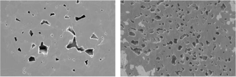
The section of shale after ion plane polishing reveals that the nano-scale pores on the sample surface are inorganic pores on the left and organic pores on the right. SEM image of petroleum geology.
SEM image of internal structure and material characteristics of mobile phone flexible screen after ion cutting, semiconductor field.
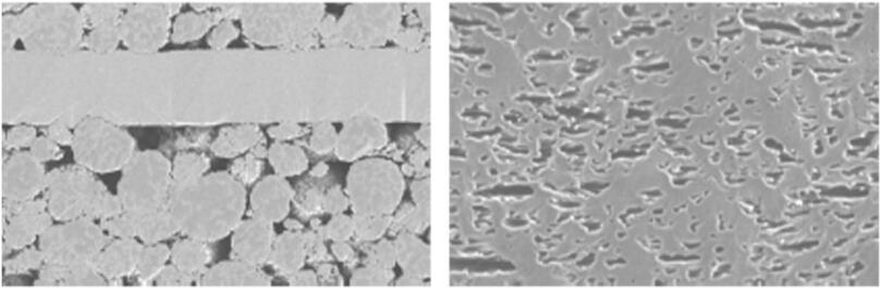
The cross-section of the battery material after ion cutting reveals its internal structure. The left picture showing the anode plate of the battery, the right picture showing the battery diaphragm, the SEM image, and the field of energy battery materials.

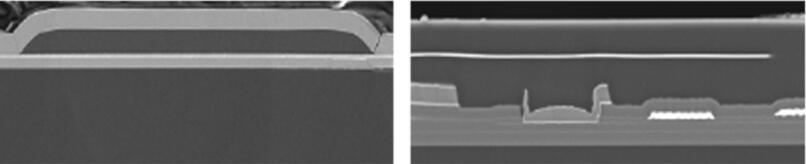
The left figure showing the internal structure of the chip after ion cutting, the right figure showing the internal structure of the chip after ion plane polishing, and the SEM image semiconductor chip field.
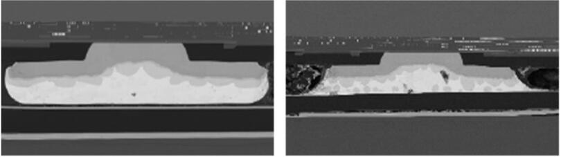
LED pad structure after plane polishing, SEM image, semiconductor optoelectronic field.
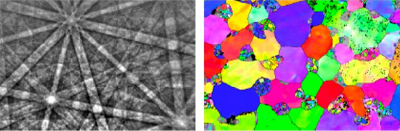
EBSD results of synthetic materials after low voltage plane polishing, EBSD image, new material field.
-
About us
Company Introduction Expert team Talent recruitment Contact us -
Products
geological prospecting Environmental Engineering Biomedical Engineering Pretreatment for SEM Archaeology/Explosion Protection -
Testing services
Field Determination of Rock Water Content Custer isotope Gold pipe hydrocarbon simulation experiment Calculation of in-situ gas content of shale Methane isothermal adsorption test Determination of Apparent Permeability of Dense Rocks -
News
Company News Industry News Technical articles Industry popsci -
Contact Us
Address:Building 101park16, No. 158 Jinfeng Road, High tech Zone, Suzhou City, Jiangsu Province Contacts:Tang Wenhao 14757974331 / 0512-68786805 Contacts:Zhao Hongxia (Sales Director) 18662204939 Email:info@guande-tech.com
